CASES
BGA package underfill
1. Challenges
High reliability requirements of aerospace and navigation, motor vehicles, automobiles, outdoor LED lighting, solar energy and military industrial electronic products, solder ball array devices on circuit boards (BGA/CSP/WLP/POP) and special devices are facing micro The trend of miniaturization is that thin PCBs with a board thickness of less than 1.0 mm or flexible high-density assembled substrates, and solder joints between devices and substrates become very fragile under mechanical and thermal stress.
Second, the solution
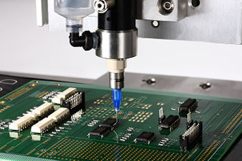
For BGA packaging, Kane KY provides an underfill process solution-an innovative capillary flow underfill. Distribute the filler to the edge of the assembled device, use the "capillary effect" of the liquid to make the glue penetrate and fill the bottom of the chip, and then heat the filler to the chip substrate, solder joints and PCB substrate.

Process advantages:
1. High fluidity, high purity, one-component, extremely fine-pitch components, fast filling, fast curing ability;
2. It can form a uniform underfill layer without voids, which can eliminate the stress caused by the welding material, improve the reliability and mechanical performance of the components, and provide good protection for the product's drop, twist, vibration, moisture, etc.
3. The system can be repaired, and the circuit board can be used again, which greatly saves costs.


